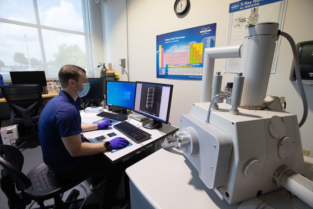
The Characterization Laboratory contains a range of equipment, including a Scanning Electron Microscope (SEM) with a spacious chamber for visualizing structural materials, which is accessible to university students, faculty and staff, as well as to external users in need of microscopy services.
Provided by an NSF MRI grant, the scanning electron microscope (SEM) is a characterization equipment used to analyze materials and devices down to the nanoscale (up to 1,000,000x at a resolution of 3 nm). SEMs can be used to analyze metals, ceramics, polymers and biomaterials. This state-of-the-art SEM can operate in high-vacuum or in environmental mode (necessary to characterize hydrated and biological specimens). Typical samples include: bulk materials, both polished and fracture surfaces; whole components; thin films; and powders.
SEM imaging and analysis capabilities in MicaPlex include: secondary electron (SE), backscatter electron (BSE) and topographic BSE imaging; elemental analysis using energy dispersive spectroscopy (EDS); and crystallographic orientation/phase analysis using electron backscatter diffraction (EBSD). The SEM large chamber allows for the visualization of structural materials installed in small test frames for in-situ experiments. The laboratory is also equipped with an optical microscope for preliminary visualization, a micro-hardness/micro-indenter and an argon environment-controlled sputter coater for non-metallic sample preparation.
Equipment
- FEI Quanta 650 Scanning Electron Microscope
- Bruker Quantax 200 Energy Dispersive Spectroscopy
- Bruker Quantax 400 Electron Backscatter Diffraction
- Bruker X-ray micro-CT scanner
- Wilson® Tukon™ 1102 Micro-Indenter
- Cressington 108 Sputter Coater with high-purity argon gas
- Olympus GX41 Inverted Microscope, 5x, 10x, 50x and 100x
Lab Information
Location: MicaPlex 111A
Lab Director: Dr. Alberto MelloContact Us: To speak to someone about this lab or any of our facilities, call us at 386-226-6100 or 800-862-2416, or email DaytonaBeach@erau.edu.
Photos